Silicon Architecture
Chip block diagram, tamper-mesh topology, Physical Unclonable Function entropy, and hardware key isolation — the layers that make Bastionchip a genuine root of trust.
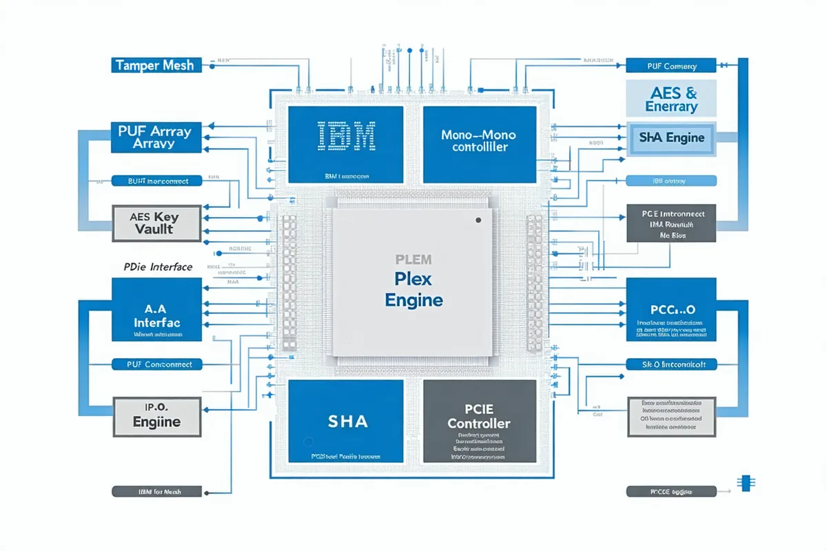
Full chip architecture
The Bastionchip die integrates all security-relevant silicon blocks into a single package. No external bus exposure of key material.
Active detection, not passive marking
Bastionchip's tamper mesh is not a passive security seal. It is an active metal structure continuously monitored for integrity. Any attempt to probe, delayer, or inject power is detected in hardware without requiring an external stimulus.
-
Sub-nanosecond zeroize. Key material erased from all storage elements in under 1 ns after tamper detection.
-
Cryptographic tamper log. Every tamper event is signed and stored in a hardware log readable by authorized auditors.
-
Always-armed. Mesh monitoring operates even at minimum power levels. No window of vulnerability during power transitions.
-
Side-channel hardening. RTL-level countermeasures against timing analysis, power analysis, and electromagnetic side-channel attacks.
Device identity from silicon randomness
Each Bastionchip die contains a PUF cell array that exploits manufacturing variation at the transistor level to derive a unique, reproducible device key. The key cannot be extracted from the die, cannot be cloned, and is never stored persistently.
Because no factory key injection is required, the Bastionchip supply chain has no key-injection attack surface. The device identity is created the first time the chip powers on, using entropy that exists nowhere else in the universe.
View full PUF specificationsTechnical architecture review
NDA-gated architecture deep-dive available for qualified cloud, financial, and defense security teams. Full RTL architecture documentation on request.