Bastionchip silicon in evaluation — now accepting qualified partner requests. Request Eval Kit →
Bastionchip Platform / HSM

HSM Silicon

Discrete security element with dedicated crypto engine, active tamper-detection mesh, and internal key storage that never traverses external buses.

AES-256-GCM 10 Gbps
Specifications

HSM die electrical and functional specifications

ParameterValue
Process node28 nm HPC (high-performance CMOS)
Die size (target)4.2 mm × 4.2 mm
Supply voltage1.0 V core / 1.8 V I/O
Operating temp−40°C to +85°C (industrial grade)
AES-256-GCM throughput10 Gbps (hardware pipeline)
SHA-3/512 throughput5 Gbps
ECDSA P-384 ops12,000 sign/verify per second
Kyber-768 encapsulation8,000 ops/second
Key storage2048 key slots, 256-bit keys, no external bus access
PUF entropy256-bit device root key, NIST SP 800-90B-aligned entropy source
Host interface (primary)PCIe x4, Gen 3 (32 Gbps bandwidth)
Host interface (secondary)SPI Mode 0/3, up to 50 MHz
Management interfaceI2C, 400 kHz fast mode
Standby power<5 μW (zeroize circuit armed)
Active power<1.2 W at full crypto throughput
Tamper meshActive metal mesh, <1 ns zeroize response
Tamper events loggedCryptographically signed tamper log, non-volatile
PackageBGA-256, 12 mm × 12 mm, 0.8 mm pitch
FIPS 140-3 targetLevel 3 (physical security)
Driver supportLinux 5.15+, UEFI 2.10, Windows Server 2022+
Block Diagram

HSM die internal architecture

HSM silicon die block diagram with crypto engine, key storage, tamper mesh, and host interface sections clearly delineated
Applications

Where HSM silicon is deployed

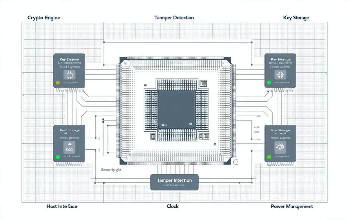
Cloud Key Management

PCIe-attached HSM on host servers, providing hardware-backed key operations for cloud key management service deployments. Replaces software HSM emulation and network HSM appliances with a silicon-level trust anchor co-located with workloads.

Financial Cryptography

Designed for FIPS 140-3 Level 3 and PCI-HSM key custody requirements — payment processing, PIN block encryption, and digital asset custody. Silicon-native deployment co-located at the processing node eliminates the centralized failure surface of network HSM appliances.

Request HSM silicon evaluation

Evaluation kits available for qualified design partners. NDA required. Full datasheet package on request.